

Войти Присоединиться бесплатно


1 / 3
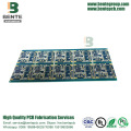
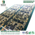
Tg170 HDI PCB ITEQ
| Brand Name : | BentePCB |
|---|---|
| Type : | Rigid Circuit Board |
Shenzhen, Guangdong, China
- Дистрибьютороптовик
- Производитель
- Услуга
- OEM -сервис
- Сертификация платформы

- Сертификация SGS

- Пояс и дорога

- видео


Описание продукта
Product Description:
8 Layers HDI PCB can be used in Medical Equipment, Process Characteristics are Line Spacing is Small and Thick Gold, Minimum BGA pad is 0.22mm, Thickness is 1.8mm, Finished Copper is 1oz, Surface Treatment is ENIG 3u.
Put the printed board on the test platform, the test pin is inserted into the place where the warp is the most, to test the diameter of the pin, divided by the length of the curved edge of the printed board, the printed board can be calculated Curvature.
Good News: Every orders will get free SMT stencil , please check out our website at www.bentepcb.com/onlinepcb.htm
HDI PCB:
High Density Interconnects (HDI) are used to meet the market demand for complex designs in smaller form factors across the majority of market segments, (Wireless, Telecom, Military, Medical, Semiconductor, and Instrumentation).
HDI Circuit boards, one of the fastest growing technologies in PCBs, HDI Boards contain blind and/or buried vias and often contain microvias of .006 or less in diameter.
They have finer lines and spaces always = <3mil They have a higher circuitry density than traditional circuit boards.
Andwin maintains years of experience with HDI products and was a pioneer of second generation microvias. now offer an entire family of microvia technology solutions for your next generation products.
Stack up of HDI PCB
Stack up of 1 Step HDI PCB

Stack up of 2 step HDI PCB

Stack up of 2 steps HDI with blind via and buried via

Anylayer connect of HDI PCB, need to adjust drill

About Us:
BentePCB is a professional PCB manufacturing which is focus on double side, multilayer, HDI PCB, rigid PCB and flexible PCB mass production. The company was established on 2011.
We have two factories together, The factory in Shenzhen is specialized in small and middle volume orders and the factory in Jiangxi is for big volume.
Why Us?
UL (E492586), ISO9001, ISO14001, TS16949, RoHS certified.
Turnover USD 10-50 million per year.
15,000 sqm area, 450 staff .
Mass Production from single to 16 layers.
Special Material:ROGERS, Arlon, Taconic.etc.
Client:Huawei, SAMSUNG, Malata, Midea,Texas Instruments.etc.
Certification(UL:E492586, TS16949, ISO14001, ISO9001,RoHS):


Factory Tour:


Exhibition:
We Took part in the famous exhibitions over the past years,and got highly appreciation from the top experts,as well as cooperated tightly with them.

Delivery:
BentePCB offers flexible shipping methods for our customers, you may choose from one of the methods below.


We don`t just sell PCBs .We sell sleep.

Shenzhen, Guangdong, China
- Дистрибьютороптовик
- Производитель
- Услуга
- OEM -сервис
- Сертификация платформы
- Сертификация SGS
- Пояс и дорога
- видео
Отправьте запрос этому поставщику